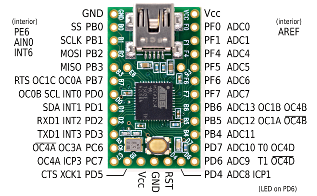
MEAM.Design - Teensy - Board Pinout & Functionality

Pinout of Teensy2.0 from www.pjrc.com
Left Side
| GND | GND | board ground |
| B0 | B0 | GPIO port B, bit 0 |
| PCINT0 | pin-change interrupt, channel 0 | |
| SS | SPI slave select | |
| B1 | B1 | GPIO port B, bit 1 |
| PCINT1 | pin-change interrupt, channel 1 | |
| SCLK | SPI bus serial clock | |
| B2 | B2 | GPIO port B, bit 2 |
| PCINT2 | pin-change interrupt, channel 2 | |
| MOSI | SPI master-out/slave-in | |
| B3 | B3 | GPIO port B, bit 3 |
| PCINT3 | pin-change interrupt, channel 3 | |
| MISO | SPI master-in/slave-out | |
| B7 | B7 | GPIO port B, bit 7 |
| PCINT7 | pin-change interrupt, channel 7 | |
| OC0A | output compare 0A | |
| OC1C | output compare 1C | |
| /RTS | UART flow control | |
| D0 | D0 | GPIO port D, bit 0 (pulled up by a 2.2k resistor) |
| OC0B | output compare 0B | |
| SCL | I2C (TWI) clock | |
| INT0 | External Interrupt, channel 0 | |
| D1 | D1 | GPIO port D, bit 1 (pulled up by a 2.2k resistor) |
| SDA | I2C (TWI) data | |
| INT1 | External Interrupt, channel 1 | |
| D2 | D2 | GPIO port D, bit 2 |
| RXD1 | USART receive | |
| INT2 | External Interrupt, channel 2 | |
| D3 | D3 | GPIO port D, bit 3 |
| TXD1 | USART transmit | |
| INT3 | External Interrupt, channel 3 | |
| C6 | C6 | GPIO port C, bit 6 |
| OC3A | output compare 3A | |
| /OC4A | inverted output compare 4A | |
| C7 | C7 | GPIO port C, bit 7; pull-up optional; high sink/source |
| ICP3 | Input capture, channel 3 | |
| OC4A | output compare 4A |
Right Side
| V+ | 5V | main power for the board, usually 5V (when connected to USB, you should disconnect this power source) |
| F0 | F0 | GPIO port F, bit 0 |
| ADC0 | analog-to-digital converter, channel 0 | |
| F1 | F1 | GPIO port F, bit 1 |
| ADC1 | analog-to-digital converter, channel 1 | |
| F4 | F4 | GPIO port F, bit 4 |
| ADC4 | analog-to-digital converter, channel 4 | |
| F5 | F5 | GPIO port F, bit 5 |
| ADC5 | analog-to-digital converter, channel 5 | |
| F6 | F6 | GPIO port F, bit 6 |
| ADC6 | analog-to-digital converter, channel 6 | |
| F7 | F7 | GPIO port F, bit 7 |
| ADC7 | analog-to-digital converter, channel 7 | |
| B6 | B6 | GPIO part B, bit 6 |
| PCINT6 | pin-change interrupt, channel 6 | |
| ADC13 | analog-to-digital converter, channel 13 | |
| OC1B | output compare 1B | |
| OC4B | output compare 4B | |
| B5 | B5 | GPIO port B, bit 5 |
| PCINT5 | pin-change interrupt, channel 5 | |
| ADC12 | analog-to-digital converter, channel 12 | |
| OC1A | output compare 1A | |
| /OC4B | inverted output compare 4B | |
| B4 | B4 | GPIO port B, bit 4 |
| PCINT4 | pin-change interrupt, channel 4 | |
| ADC11 | analog-to-digital converter, channel 11 | |
| D7 | D7 | GPIO port D, bit 7 |
| T0 | Timer 0 external clock input | |
| ADC10 | analog-to-digital converter, channel 10 | |
| OC4D | output compare 4D | |
| D6 | D6 | GPIO port D, bit 6; connected to RED led (high = on) |
| T1 | Timer 1 external clock input | |
| ADC9 | analog-to-digital converter, channel 9 | |
| /OC4D | inverted output compare 4D |
Bottom Row
| D5 | D5 | GPIO port D, bit 5 |
| XCK1 | USART external clock in/out | |
| /CTS | UART flow control | |
| V+ | 5V | main power for the board, usually 5V (when connected to USB, you should disconnect this power source) |
| GND | GND | board ground |
| RST | Reset | Active low reset line - also tied to reset switch. |
| D4 | D4 | GPIO port D, bit 4 |
| ICP1 | Input capture, channel 1 | |
| ADC8 | analog-to-digital converter, channel 8 |
Internal
| E6 | E6 | GPIO port E, bit 6; |
| INT6 | external interrupt, channel 6 | |
| AIN0 | analog comparator positive input | |
| ARef | ARef | analog reference voltage |